

Introduction to the Quantum Theory of Solids II
Introduction: Extension to Three Dimensions
In the preceding article, we developed a basic understanding of allowed and forbidden energy bands. Here, we extend those concepts to three dimensions and real crystals. We will discuss the distinctive characteristics of three-dimensional crystals qualitatively through E-k diagrams, band-gap energy, and effective mass. Once again, advanced details are omitted; our aim is to give readers a sound foundation in these concepts.
Extending the potential to three dimensions presents a difficulty: the interatomic spacing varies with direction in the crystal. Electrons traveling in different directions encounter different potential patterns and therefore different k-space boundaries. To understand the crystal, we will examine energy diagrams as a function of k-space direction.
k-Space Diagrams: Si and GaAs
Recall that in semiconductor physics, an electron’s behavior is determined not only by its energy () but also by its wave vector () in the crystal lattice. In quantum mechanics, is directly proportional to the electron’s crystal momentum ().
- Energy–Momentum Relation: The diagram maps how an electron’s energy varies with momentum as it moves through the allowed energy bands—the valence and conduction bands.
- Physical Significance: The effective mass () of electrons and holes is derived from the curvature of an energy band (). These diagrams allow direct analysis of electrical conductivity, optical absorption/emission, and carrier mobility.
Before examining the diagrams, let us briefly discuss direct and indirect transitions, a distinction essential to understanding semiconductors. The key is conservation of momentum.
-
Direct Transition
The conduction-band minimum and valence-band maximum occur at the same , generally , the point. An electron drops to the valence band in a single step. Although photons carry high energy, their momentum () is negligible relative to an electron’s, so no momentum change occurs (). The energy is emitted directly as a photon. The process is very fast and optically efficient.
-
Indirect Transition
The conduction-band minimum and valence-band maximum occur at different values. In moving to the lower band, the electron must lose energy and undergo a large position/momentum shift. Because a photon cannot supply the momentum change, a phonon—a crystal-lattice vibration, or quantum of vibrational/thermal energy—must participate. This three-way electron–photon–phonon process is much less probable. Most of the energy becomes heat, in the form of phonon–lattice vibration, rather than light.
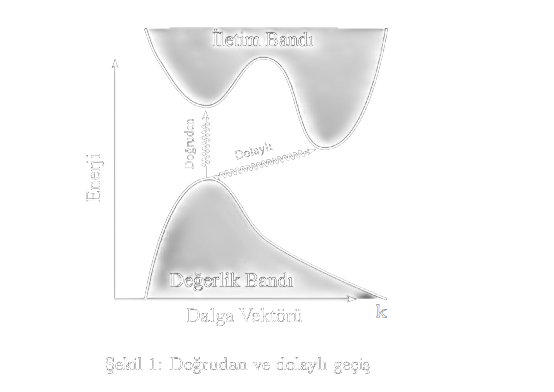
Figure (2) shows the E-k diagrams of gallium arsenide (GaAs) and silicon (Si). In GaAs, the valence-band maximum and conduction-band minimum occur at exactly the same , namely . Conduction electrons collect at the minimum there, while valence-band holes collect at the maximum. Since the transition requires no momentum change, GaAs is an ideal direct-band-gap material for LEDs, semiconductor lasers, and optoelectronic devices. In silicon, the conduction-band minimum lies away from along [100], while the valence-band maximum is at . Because interband transitions require a phonon-assisted momentum change, Si emits light very inefficiently. Its suitable band gap, native oxide layer (), and excellent electrical properties nevertheless make it the basic material for microprocessors, integrated circuits, and solar cells. Rather than conventional positive and negative axes, the E-k plot shows two crystal directions. Since the one-dimensional E-k diagram is symmetric about , repeating the negative axis adds no information. Conventionally, [100] is drawn to the right and [111] to the left. In diamond or zinc-blende structures, the valence-band maxima and conduction-band minima occur either at or along these directions.
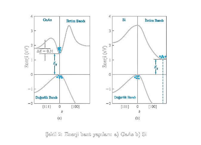
Like silicon, germanium (Ge) is an indirect-band-gap semiconductor. Its valence-band maximum occurs at , while its conduction-band minimum lies along [111]. Thus, a phonon must participate to conserve momentum in germanium’s interband transitions.
Effective-Mass Concepts
An electron generally moves differently in a crystal lattice than in free space. Its motion is governed not only by an externally applied force, but also by internal crystal forces from positively charged ions, or protons, and other negatively charged electrons. The total force on a particle in the crystal () is the sum of the applied external force () and the internal forces ():
Here, is the particle’s acceleration and its rest mass. Since accounting separately for every internal force is extremely difficult, the equation can be simplified to relate the external force directly to acceleration:
The parameter is called the effective mass. It combines the particle’s bare mass and the total effect of its complex crystal interactions into one quantity.
The curvature of the curve near the conduction-band minimum is directly related to the electron effective mass :
In quantum mechanics and semiconductor physics, the electron effective mass for a one-dimensional model is defined by
Second Derivative (): This measures the curve’s curvature. The greater the curvature—the steeper or narrower the graph—the larger the second derivative and hence the smaller the effective mass . Returning to Figure (2), the curvature at the GaAs conduction-band minimum is very large, forming a sharp valley; therefore, a conduction electron in GaAs has a smaller effective mass.
The curvature at silicon’s conduction-band minimum is broader and flatter, so electrons in Si have a larger effective mass than those in GaAs. Electrons with smaller effective mass respond more rapidly to an electric field and have greater mobility. This low effective mass is one principal reason GaAs is preferred for high-frequency, high-speed circuits.
Density-of-States Function
To determine the current–voltage () characteristics of semiconductor devices, we must know the numbers of free electrons and holes, or carriers, in the crystal. Calculating carrier populations depends directly on the density-of-states (DoS) function. Pauli Principle and Energy Levels: Under the Pauli exclusion principle, only one electron may occupy a particular quantum state. Thus, the number of electrons contributing to conduction is limited by the number of available states. Although energy bands appear continuous, they consist of discrete levels separated by very small intervals. Our immediate aim is to determine the density per unit volume, , of these allowed quantum states as a function of energy so that electron and hole concentrations can be calculated.
Mathematical Derivation
To calculate the energy-dependent density of allowed quantum states, we need an appropriate mathematical model. Although electrons can move relatively freely in a semiconductor’s conduction band, they remain confined within the crystal. We therefore begin with a free electron confined in a three-dimensional infinite potential well representing the crystal. Its potential is defined as
We assume the crystal is a cube of side length . The three-dimensional Schrödinger equation can be solved by separation of variables.
Using the one-dimensional infinite-well result, in three dimensions we can show:
In Terms of the Components of the Wave Vector ():
After applying boundary conditions, in terms of the quantum numbers () and cube side ():
This gives the form above, where are positive-integer quantum numbers.
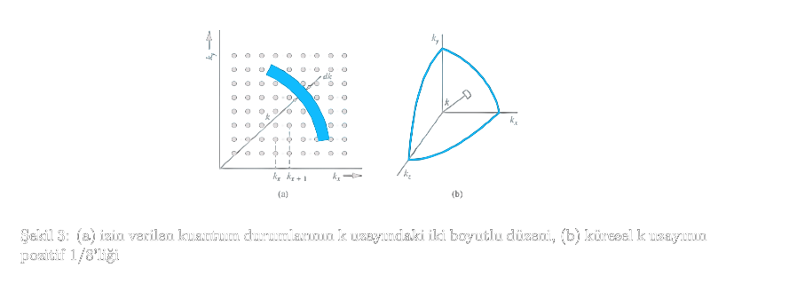
Negative values of , , and produce wave functions with the same probability function and energy as the corresponding positive integers, differing only in sign; they therefore do not represent distinct quantum states. The allowed states can be plotted schematically in -space. Figure (3.a) is a two-dimensional plot in and , with each point representing an allowed state corresponding to integer values of and . Positive and negative values of , , or have the same energy and represent the same energy state. Since negative values do not create additional states, the state density can be determined using only the positive one-eighth of spherical -space, as in Figure (3.b). For example, the spacing between adjacent states along is
Generalizing to three dimensions, the volume occupied by one quantum state is
as shown.
We can now determine the density of quantum states in -space. A differential volume, shown in Figure 3.b, is . Thus, the differential density of states in -space is
Figure (3.a) Two-dimensional arrangement of allowed quantum states in -space. (b) The positive one-eighth of spherical -space.
The first factor, , accounts for the two spin states allowed for each quantum state, spin-up and spin-down. The factor indicates that only states with positive are counted. The factor is the differential shell volume, and is the volume of one quantum state. Simplifying gives
Equation 8 gives the state density as a function of momentum through . We can now express it in terms of energy . For a free electron, the relation between and is
or
Hence the differential is
Substituting and into equation (8), the number of states between energies and is
Since , the equation becomes
Equation 13 gives the total number of states between and in the crystal’s total volume . Dividing by gives the density of quantum states per unit volume:
The state density is a function of energy . As the free electron’s energy decreases, the number of available states also decreases. This is actually a “double density,” measured as the number of states per unit volume per unit energy, or .
Extension to Semiconductors
We have derived a general expression for the density of allowed states using a free electron of mass confined in a three-dimensional infinite potential well. We can extend this model to a semiconductor to determine the densities of states in its conduction and valence bands. Since electrons and holes are confined within the semiconductor crystal, we again use the basic infinite-well model.
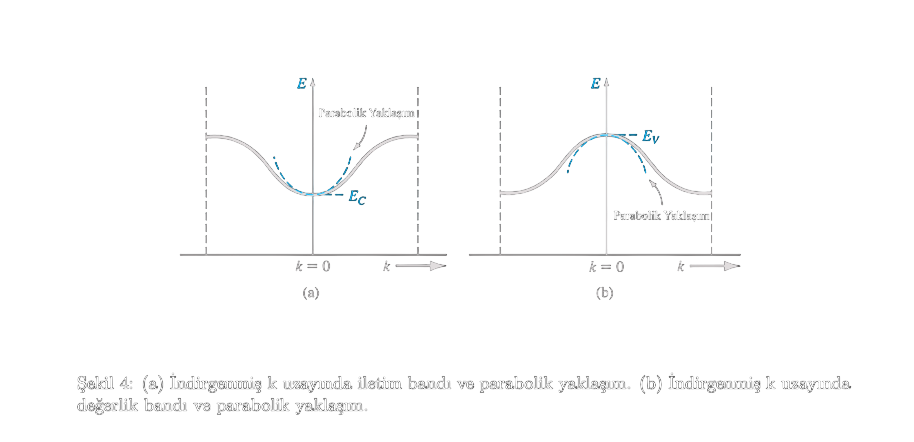
The parabolic relation between a free electron’s energy and momentum was . Figure 4.a shows the conduction-energy band in reduced -space. Near , the curve at the bottom of the conduction band () can be approximated by a parabola, so
Here, is the lower edge of the conduction band and is the electron density-of-states effective mass.
For an electron at the bottom of the conduction band, the general relation is the same as for a free electron except that mass is replaced by effective mass . We can therefore regard the electron there as a “free” electron with its own characteristic mass.
The right side of equation 15 has the same form as the equation used to derive the density-of-states function, . Using this similarity—the “free” conduction-electron model—we can generalize equation 14 and write the allowed electronic density of states in the conduction band as
This is valid for . As the conduction electron’s energy decreases toward , the number of available states decreases. The valence-band density of states follows from the same infinite-well model because a hole is confined in the semiconductor crystal and can be treated as a “free” particle. Its density-of-states effective mass is . Figure 4.b shows the valence-energy band in reduced -space. Near , the curve for a “free” hole can again be approximated by a parabola:
Rearranging equation (17) gives
Again, the right side of equation (18) has the form used in the general density-of-states derivation. We can therefore generalize equation (14) to the valence band:
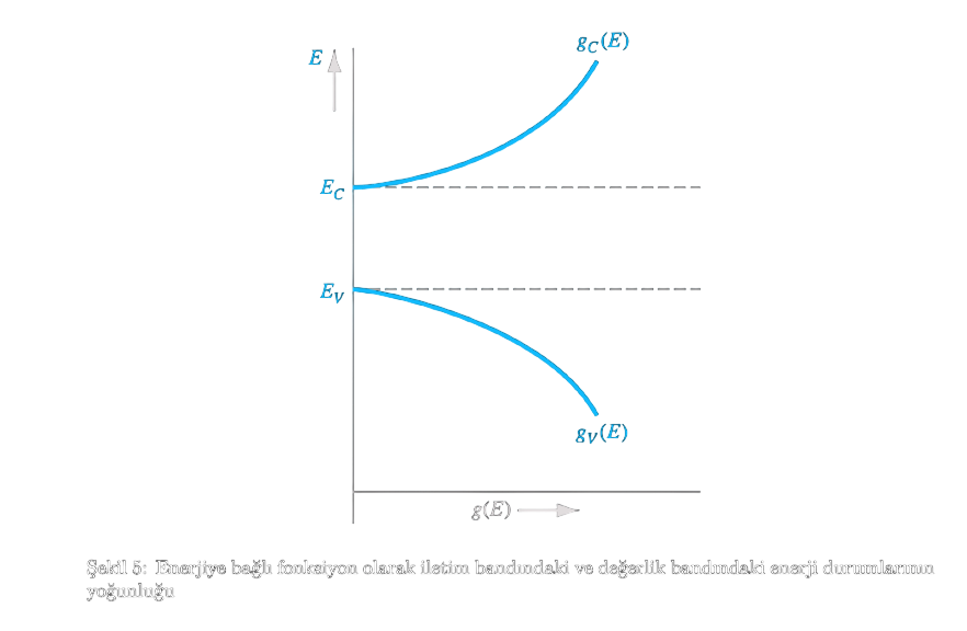
Equation (3.75) is valid for . There are no quantum states within the forbidden band gap, so for . Figure 5 plots the density of states against energy. If electron and hole effective masses were equal (), and would be symmetric about the midgap energy , halfway between and .
Statistical Mechanics
When studying systems of many particles, we consider the statistical behavior of the ensemble rather than the behavior of every individual particle. When particle numbers are extremely large, calculating each particle’s interactions and motion is neither practical nor necessary.
As in fluid mechanics, the observed electrical properties of crystals are determined by the collective statistical behavior of enormous numbers of electrons. Let us briefly consider several statistical distribution laws.
Statistical Laws
To determine an ensemble’s statistical behavior, we must first know which statistical law its particles obey. Three fundamental distribution laws describe how particles are distributed among available energy states.
- Maxwell–Boltzmann Distribution: Particles are assumed distinguishable and noninteracting; each particle is distinct. There is no upper limit on the number occupying one energy state. Molecules in a low-pressure gas are a good example.
- Bose–Einstein Distribution: Particles are indistinguishable and noninteracting, meaning they are completely identical and it is physically meaningless to distinguish which particle occupies which state. There is no limit on the number sharing one quantum state. Photons and blackbody radiation obey this distribution.
- Fermi–Dirac Distribution: Here too particles are indistinguishable and noninteracting, but unlike in Bose–Einstein statistics, at most one particle may occupy each quantum state. This restriction follows directly from the Pauli exclusion principle. Electrons in a crystal obey Fermi–Dirac statistics.
The common assumption in all three distributions is that the particles do not interact. As discussed above, deviations caused by this assumption can be corrected through concepts such as effective mass.
Using Fermi–Dirac statistics, let us see how electrons in a semiconductor are distributed among quantum states.
Fermi–Dirac Probability Distribution Function
Figure 6 shows the th energy level containing quantum states. Suppose we wish to place electrons at this energy level.
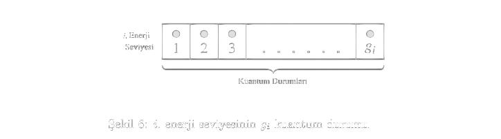
Accounting for the Pauli exclusion principle and the indistinguishability of electrons, the number of ways to place electrons among the states at level is given by the repeated permutation below.
Equation (20), however, applies to one energy level. If the system has levels, multiplying the independent numbers of arrangements at each level () gives the system’s total number of arrangements:
Here, is the total number of distinct ways in which the system’s electrons can occupy all energy levels.
The total number of electrons is
as written above.
The central aim of statistical mechanics is to find, among all possible arrangements, the most probable distribution—in this example, the distribution maximizing W. Holding the total electron number and total system energy fixed produces the Fermi–Dirac distribution function :
is the number density, a function giving the particle count per unit volume per unit energy. is the number of quantum states per unit volume per unit energy. is the Fermi energy, and is Boltzmann’s constant.
- Fermi energy: The energy of the highest occupied quantum state in an equilibrium system at T = 0 K.
Equation (23), one of solid-state physics’ most fundamental results, gives the probability that a quantum state at energy is occupied by an electron.
Distribution Function and Fermi Energy
To understand the distribution function better, we can plot it against energy . First consider in the limit. The exponential in equation (23) approaches zero, so . If at , the exponential tends to positive infinity and . Figure 7 shows the resulting distribution.
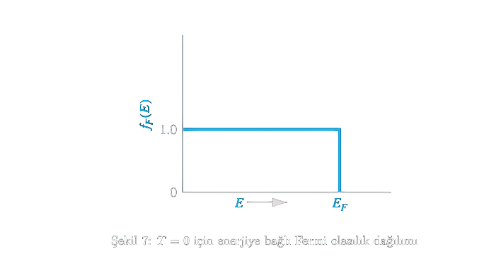
The conclusion is that at absolute zero (), electrons fill the lowest available energy levels. A state with is occupied with certainty, while one with has zero probability of occupation. In other words, at absolute zero every electron has energy below the Fermi energy.
An important distinction is needed here. We defined the Fermi energy above. Many textbooks use “Fermi level”—or, more commonly, chemical potential —and “Fermi energy” synonymously, which can cause confusion. The Fermi energy is fundamentally the specific value the Fermi level takes at absolute zero. Fermi energy relates to energy eigenvalues, whereas the Fermi level is a statistical reference energy for the entire thermodynamic system and need not be an actual energy level in the system. As we will see, this distinction explains why the Fermi level can lie in a forbidden band gap. To remain consistent with textbooks, we will continue using this conventional interchangeability; readers need only keep the distinction in mind.
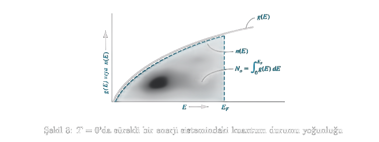
Assuming the density of states is continuous in energy, Figure 8 shows how the electrons in a system of electrons occupy quantum states at K. If and are known, can be calculated.
Now consider temperatures above absolute zero ( K).
As temperature rises, electrons acquire thermal energy from their surroundings and can move to higher energy levels. Their distribution among available states therefore differs from that at absolute zero.
When and K, the exponential in equation (23) is zero, so the distribution function becomes
as shown.
Thus, at nonzero temperature, a state at has occupation probability 0.5.
Figure 9 shows the temperature dependence of the Fermi probability function. As temperature rises, its sharp transition becomes progressively smoother. Consequently, some states above the Fermi energy have nonzero occupation probability, while some below it have nonzero probability of being empty.
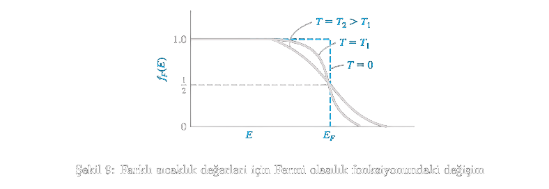
Moreover, the probability that a state above is occupied equals the probability that a state below it is empty. Thus, and are symmetric about the Fermi energy.
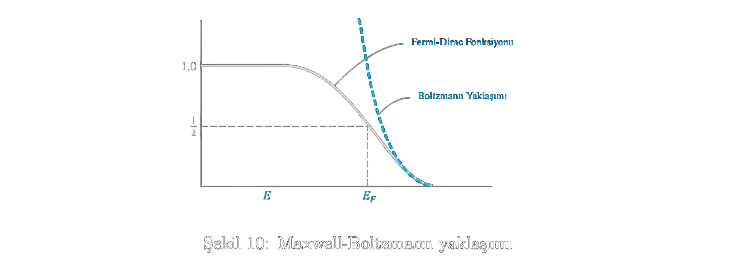
Finally, consider . The denominator in equation (23) is then much greater than one, so the 1 in the denominator can be neglected and the equation
can be rewritten as above. Equation (25) is known as the Maxwell–Boltzmann approximation and will be used in later parts.
In this article, we examined electron energy–momentum relations in crystals, introduced effective mass, derived the density-of-states function, and treated it statistically. We also defined the Fermi energy, which we will use frequently, and examined its temperature dependence.
In our next article:
- Charge carriers and electrical conduction
- Fermi energy level
- Doping and acceptor–donor statistics
will take us another step toward understanding semiconductor technologies.
References
- Semiconductor Physics And Devices by Donald A. Neamen Third Edition
- The Oxford Solid State Basics by Steven H. Simon