
Semiconductor Physics Series, Part 1—The Crystal Structure of Solids
Introduction
In the first part of our semiconductor physics series, before delving into complex equations and concepts, we will begin by examining the crystal structure of solids. Understanding how atoms are arranged is crucial to comprehending the characteristics and electronic properties of semiconductors. This introductory part presents the fundamental theoretical framework for single-crystal structures and crystal-growth techniques, which determine the electrical characteristics of semiconductor materials and devices. Let us first briefly classify semiconductor materials.
Semiconductor Materials
Semiconductor materials have conductivities between those of metals and insulators. We can classify semiconductor materials as elemental (single-element) and compound semiconductors. Elemental semiconductors are among the Group IV elements of the periodic table, whereas compound semiconductors consist of certain specific combinations of Group III and Group V elements or Group II and Group VI elements.
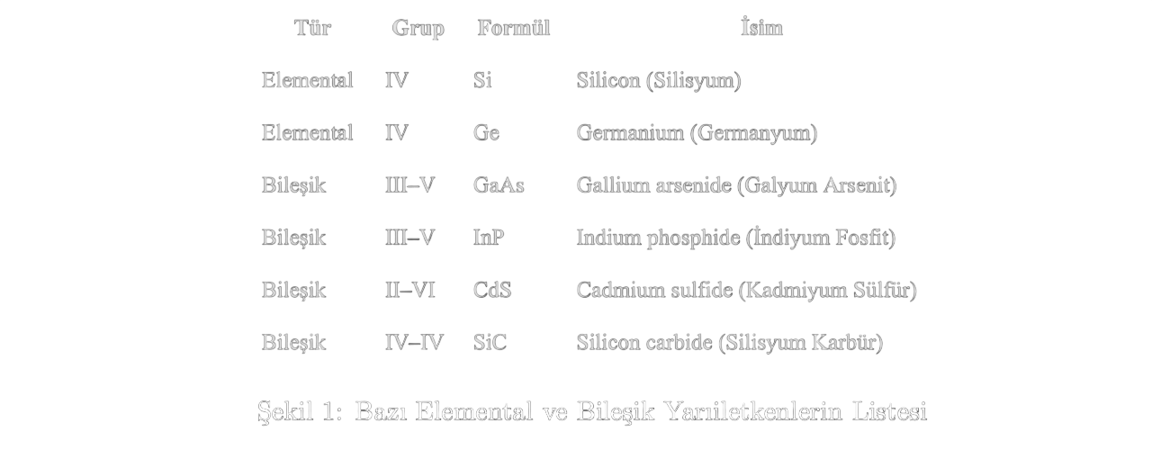
In addition to those shown in the figure, we can also form ternary compound semiconductors, for example:
More complex semiconductors that provide flexibility in the selection of material properties can also be formed.
Types of Solids
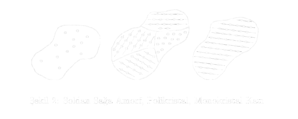
We can broadly classify solids into three types according to their structure: amorphous solids, polycrystalline solids, and single-crystal (monocrystalline) solids. The atoms in amorphous solids do not form an ordered, periodic lattice structure. There is no long-range order. Polycrystalline solids consist of many small crystal grains. Each grain is ordered internally, but their orientations differ. In single-crystal solids, the atoms form a single, continuous crystal-lattice arrangement throughout the entire structure. In other words, these single-crystal materials ideally possess a highly ordered and geometrically periodic atomic arrangement throughout their entire volume.
The most important advantage of the single-crystal structure is the absence of grain boundaries, because grain boundaries can adversely affect electrical properties. Therefore, the electrical properties of single-crystal materials are generally superior to those of non-single-crystal materials, such as polycrystalline materials. Two-dimensional representations of these three types of solids are shown in the figure below.
Lattice Geometry (Space Lattices)
To describe a crystal structure mathematically, we use a combination of two concepts:
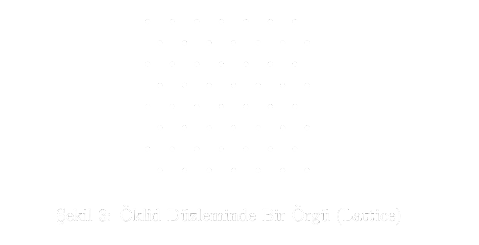
Lattice: In the language of group theory, a lattice is a discrete subgroup of the group of -dimensional Euclidean space , an infinite set of points in that space. It has the following properties:
- Adding or subtracting the coordinates of any two points in the lattice yields another lattice point.
- All lattice points are separated by a certain minimum distance.
- The neighborhood of any point in the lattice is equivalent to the neighborhood of any other point in the lattice.
Basis: In the context of a crystal structure, this is the group of atoms repeated at each lattice point.
Primitive and Unit Cells
Unit Cell: A unit cell is the fundamental repeating building block of a periodic structure. Because the three-dimensional lattice of a single-crystal solid consists of repeating, periodic groups of atoms, we can consider only the fundamental repeating unit cell rather than the entire lattice.
Primitive Unit Cell: A unit cell containing exactly one lattice point.
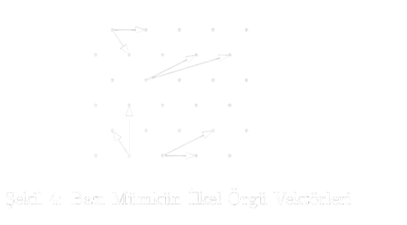
Any periodic structure can be expressed as a lattice of repeating motifs. The choice of primitive lattice vectors in a two- or three-dimensional lattice is not unique. There are infinitely many possible choices of primitive lattice vectors. At times, it may be useful to define a nonprimitive unit cell to simplify the analysis. This is called a conventional unit cell. These conventional unit cells are almost always chosen so that their axes are mutually perpendicular (orthogonal).
For two dimensions, the vector representations in the figure below can be written as
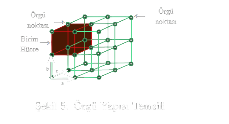
A generalized three-dimensional lattice structure and unit cell can be seen in Figure 5. We characterize the relationship between this unit cell and the lattice using vectors. Since the position of the origin is arbitrary, for simplicity we may take x, y, and z to be positive numbers.
Simple Crystal Structures
Before discussing semiconductor crystals, let us examine simple crystal structures and their properties. In the simple cubic structure, there is one atom at each corner of the cube. A body-centered cubic structure additionally contains an atom at the center of the cube; in a face-centered cubic structure, in addition to the corner atoms, there is one atom at the center of each face of the cube.
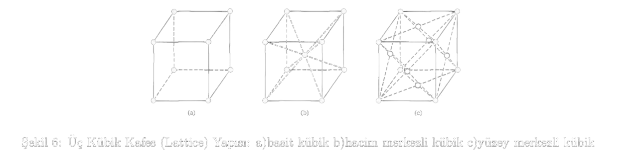
A reminder about counting lattice points in a unit cell:
In most cases, we use unit cells whose lattice points lie at the corners or on the edges of the cell.
If a lattice point lies on the boundary of the cell, it must be counted fractionally according to the portion that lies within the cell. For example, in a body-centered cubic lattice, there are lattice points at each of the 8 corners of its unit cell, of each of these points lies within the conventional unit cell, and the point at the body center is contained in its entirety; thus, the conventional cell contains a total of
lattice points. We will not discuss other, noncubic lattice structures in detail here.
Crystal Planes and Miller Indices
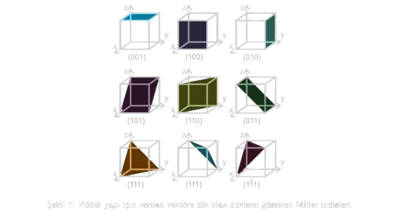
Because real crystals are finite, they ultimately terminate somewhere. Semiconductor devices are fabricated on or near a surface, so surface properties can affect device characteristics. This is critical in semiconductor manufacturing (wafer cutting). Miller indices are a notation system used to describe planes and directions within a crystal. They are written as three integers, , and, in brief, are obtained by taking the reciprocals of the points at which the plane intersects the x, y, and z axes and reducing them to integers. Thus, Miller indices are in fact the components of “reciprocal-lattice vectors.” A plane with indices is perpendicular to the vector
in the reciprocal lattice. Why do we take the reciprocals rather than using the intercepts directly? The reasons are to eliminate infinite values, represent the periodicity of the crystal, and maintain consistency with diffraction experiments (X-ray diffraction reveals the reciprocal lattice directly). If a plane is parallel to an axis, it theoretically intersects that axis “at infinity.” Taking the reciprocal converts infinities to zero, groups all parallel planes under a single “family,” and brings experimental data and theory into the same mathematical language. The , , and planes are the planes used most frequently in semiconductor technology.
Diamond Structure
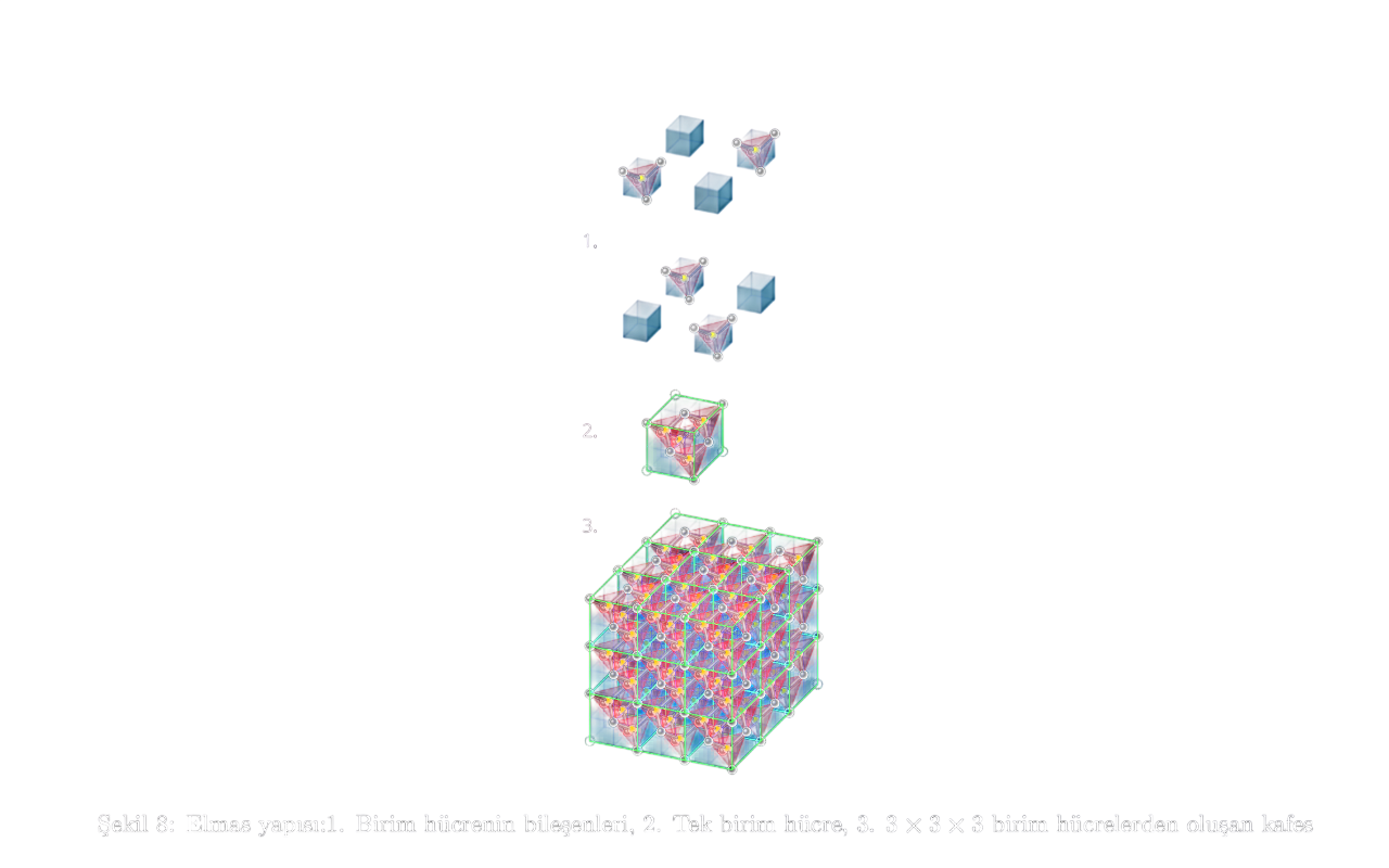
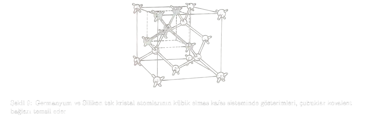
Silicon, the most common elemental semiconductor material, is a Group IV element and has the diamond crystal structure. Germanium is likewise a Group IV element with a diamond structure. The unit cell of the diamond structure is somewhat more complex than the simple cubic structures discussed thus far. Each atom in the tetrahedral structure has four nearest neighbors, and this arrangement is the fundamental building block of the diamond lattice. In other words, the diamond cubic lattice consists of atoms connected by tetrahedral bonds in each repeating primitive cell; these atoms are separated from one another by one-quarter of the cell width in each dimension of the cell.
The diamond lattice can also be viewed as the combination of two interpenetrating face-centered cubic (FCC) lattices, with one displaced from the other by one-quarter of the unit-cell width in each dimension.
Atomic Bonds
Here, we are examining various single-crystal structures. At this point, the following question arises: why is one crystal structure favored over another for a particular collection of atoms? One of the fundamental laws of nature is that the total energy of a system in thermal equilibrium tends toward the lowest possible value. The interaction through which atoms come together to form a solid structure and minimize the total energy depends on the type of atom or atoms involved. Therefore, the nature of the bond or interaction between atoms in a crystal is determined by the properties of the atoms that constitute that crystal. Without a strong bond between atoms, they cannot remain together to form a solid structure. Interactions between atoms are explained by quantum mechanics, but we leave the details to later parts. The energy bands and electrical conductivity of semiconductors arise from the periodic arrangement of these atoms and the covalent bonds they form.
Crystal Defects and Impurities
Although we may envision an ideal crystal with a flawless periodic structure, the periodicity of real crystals is disrupted by defects. This directly affects the electrical properties of the semiconductor material; indeed, the material's electrical properties can sometimes be determined entirely by creating controlled defects. We will address this later in the series when discussing “doping.”
-
Thermal Vibrations (Lattice Vibrations): The only defect common to all crystals. At every temperature above absolute zero , atoms vibrate randomly about their equilibrium positions. This causes the interatomic distance to fluctuate continuously and momentarily disrupts perfect geometrical order. In semiconductors, it affects resistance by causing charge carriers to scatter.
-
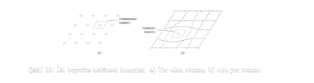
Point Defects:
Defects involving a single atom or atomic site:
Vacancy: The absence of an atom from its site in the crystal lattice.
Interstitial Atom: An atom occupying a space between normal lattice sites.
Frenkel Defect: Formed when a vacancy and an interstitial atom are close to one another and interact.
- Line Defects:
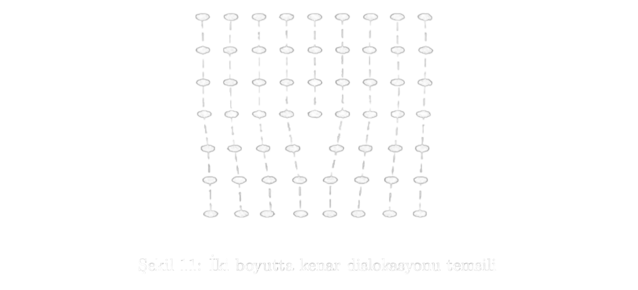
These arise when atoms are missing or incorrectly arranged along a row:
Edge Dislocation (Line Dislocation): The insertion of an extra atomic plane into the crystal structure or the complete absence of a row. Dislocations can play a constructive role in crystal growth.
These defects disrupt both geometrical periodicity and ideal chemical bonds, changing electrical properties in ways that are difficult to predict.
We will discuss the growth of semiconductor materials and growth techniques later. In Part 2, our next article, we will cover two main topics: the fundamentals of quantum mechanics and the quantum theory of solids, both of which are necessary for understanding the properties of these materials. Fasten your seat belts.
References
- Semiconductor Physics And Devices by Donald A. Neamen Third Edition
- The Oxford Solid State Basics by Steven H. Simon
- https://en.wikipedia.org/wiki/Lattice_%28group%29
- https://www.careers360.com/chemistry/crystal-lattices-and-unit-cells-topic-pge
- https://en.wikipedia.org/wiki/Diamond_cubic
- https://www.researchgate.net/figure/Miller-indices-indicating-the-plane-perpendicular-to-the-vector-given-for-the-cubic_fig7_302838100